SEMICONDUCTOR INDUSTRY
PTR EB WELDING CASE STUDIES
One of the advantages of the electron beam welding process lies in its robustness to join materials like aluminum, copper or stainless steels all commonly used by the semiconductor industry.
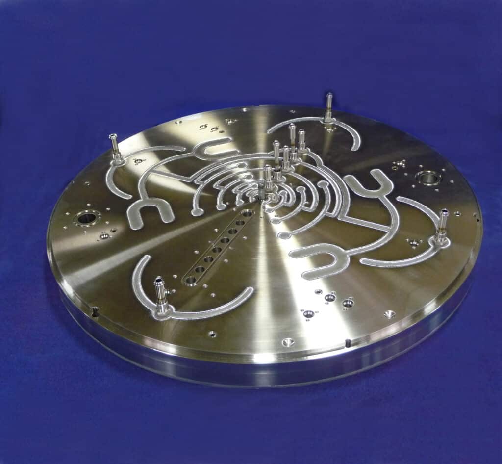
Cooling Plate Welding for Semiconductor Fab Systems
Electron Beam Welding is used to join many components in Semiconductor Fabrication equipment. In this application, gas paths are created by welding covers over milled channels. Weld geometries are typically complex, requiring CNC motion control. The low thermal distortion of electron beam welding is crucial to maintain the dimensions of the part- since all welds are located on one side of the cooling plate. EB welding is also used to attach the inlet/outlet fittings in place.
Description:
Round Plate with
Machined Cooling
Channels
Material(s):
Aluminum or Stainless
Steel
Joint Geometry:
step joint
Weld Depth:
0.200 in.
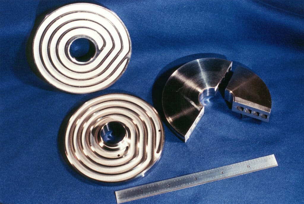
Heat Sink Welding
Used as a heat sink, this part is manufactured in machined halves which are joined together. In one of the more unique usages of electron beam welding, all the mating surfaces of this heat sink are joined in one 360° pass. Called a “tier weld”, the electron beam penetrates each of the individual joints stopping at the inner diameter wall.
Description:
5 in. diameter by 1 in.
high
Material(s):
Stainless Steel
Joint Geometry:
radial circumferential
weld
Weld Depth:
“tier weld” – multiple full
penetration welds
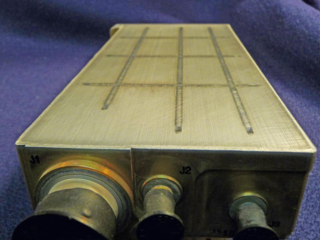
Hermetically Sealed Electronics Package Welding
Rugged metal packaging is used to protect electronic systems operating in demanding environments. The EB welding process allows weld joints to be placed in close proximity to sensitive electronic componentry without causing thermal or electrical damage. Electron beam welding is used for closure welds, creating a hermetically sealed package which can either remain under vacuum or be backfilled with an inert gas.
Description:
Metal Enclosures for
Electronics
Material(s):
Aluminum
Joint Geometry:
step joint, T, butt weld
Weld Depth:
< 0.100 in